
research · Fall 2025
MoS₂ floating-gate memory
A monolayer MoS₂ transistor with a buried platinum floating gate, studied as a non-volatile memory and a programmable resistance.
Project details
-
Charge storage in a floating gate
A floating-gate transistor stores charge in a metal gate surrounded by insulator and electrically isolated from the contacts. The stored charge shifts the voltage at which the transistor turns on. Reading that threshold provides a memory state that can persist after the external programming voltage is removed.
-
A monolayer MoS₂ channel
Molybdenum disulphide retains a band gap in a single layer and provides a thin channel whose conductance is sensitive to nearby charge. The lab project examined two uses of this device: storing distinct memory states through a threshold shift, and setting its conductance as a programmable resistance.
-
Cleanroom fabrication at CMi
Our three-person team fabricated the device at EPFL’s CMi cleanroom, using hafnium oxide insulation, a buried platinum floating gate and monolayer MoS₂. Oxygen-plasma patterning defined the channel, followed by titanium–gold contacts. I took part in both the fabrication and the electrical characterisation.
-
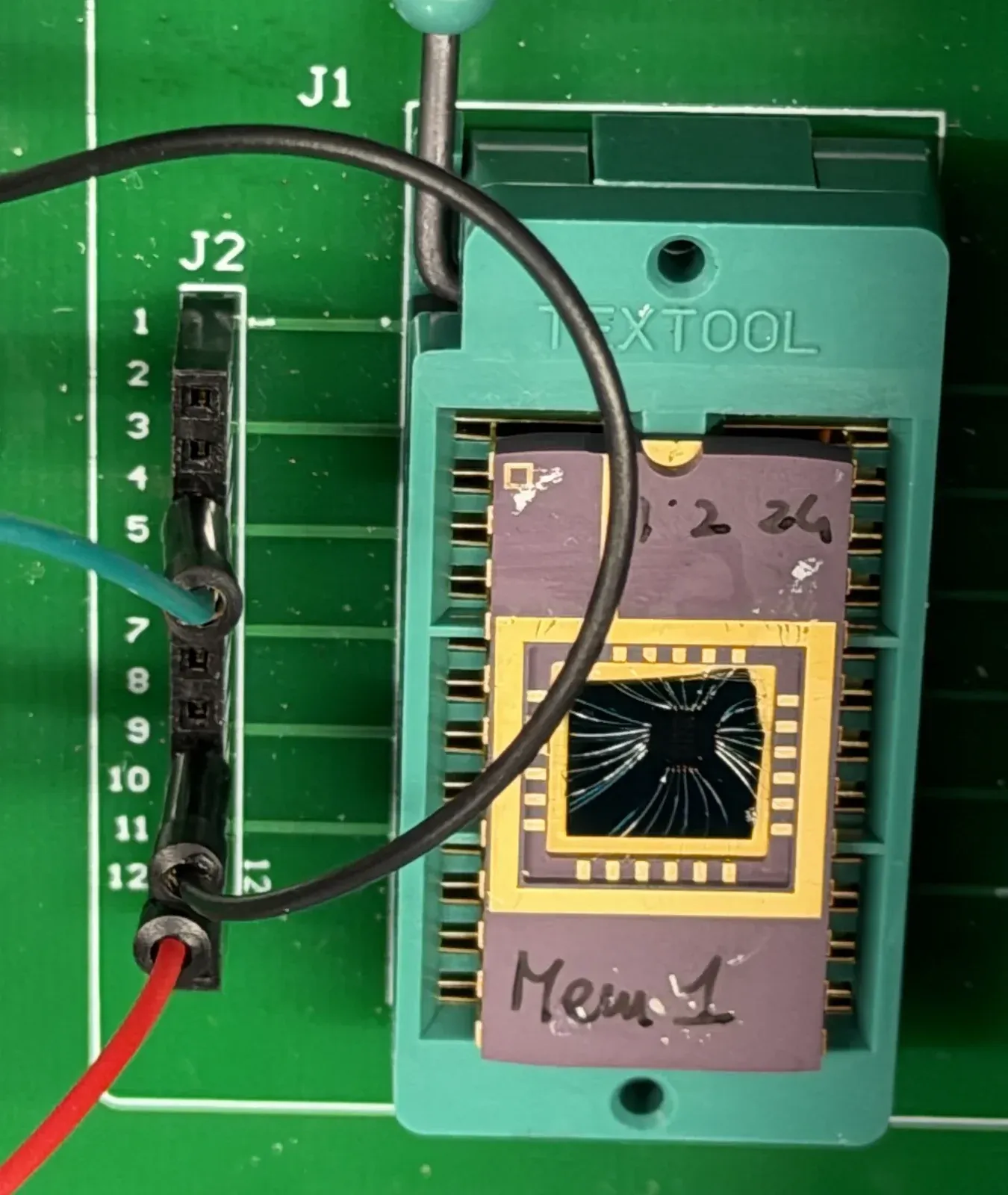
Electrical measurement setup
The chip was mounted in a zero-insertion-force socket inside a light-shielded breakout box and connected by triaxial cables to a source-measure unit with femtoampere resolution. With the drain held at 100 mV, the gate was swept from −10 V to +10 V and back. Thresholds were read at a fixed current reference.
-
Measured memory window
5.4 V between thresholds of 0.8 V and 6.2 V
The forward and reverse gate sweeps gave thresholds of 0.8 V and 6.2 V, a 5.4 V memory window consistent with charge stored in the floating gate. Published devices reach 10.6 V when swept to ±12.5 V. Our sweep stopped at ±10 V; sweep speed and oxide quality also affect this comparison.
-
Programming the channel conductance
After erasing at −10 V, sweeps to 4, 6, 8 and 10 V programmed different states. A small drain sweep gave 0.293 µS after 4 V, 0.080 µS after 6 V and nearly zero after 8 V. The intermediate states were less stable than published examples, suggesting incremental programming with verification as a useful next test.
My contribution
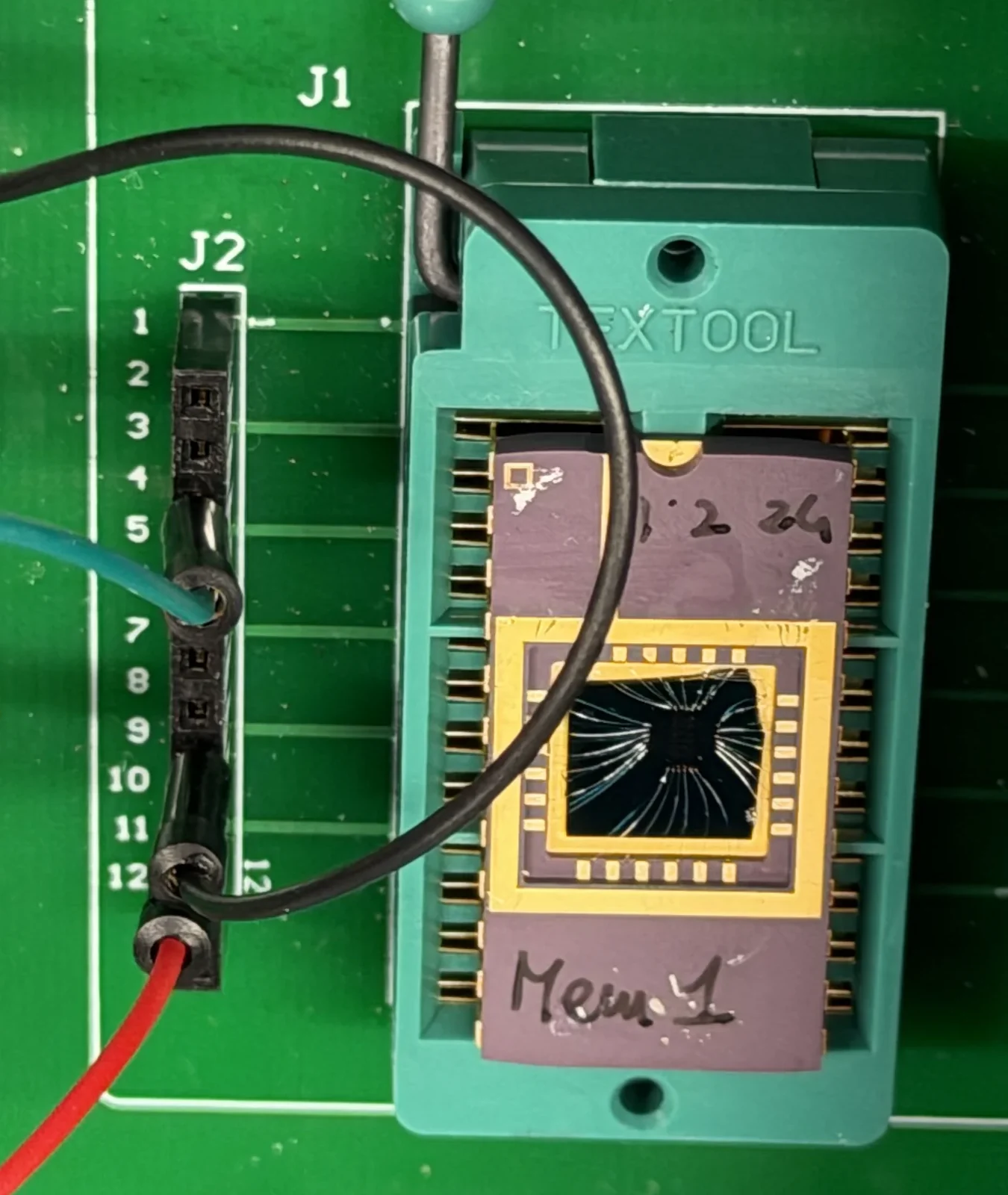
As part of a three-person team, I fabricated and characterised a MoS₂ floating-gate transistor, measuring its memory window and programmable conductance.