
research · Sept – Dec 2025
Ferroelectric gate stacks for cryogenic electronics
Hafnia-based MFMIS capacitors designed to control how voltage divides across a ferroelectric gate stack at cryogenic temperatures.
Project details
-
Ferroelectric memory for cryogenic electronics
Silicon-doped hafnium oxide can retain either of two polarisation states after power is removed. In a transistor gate, this can provide a non-volatile memory function. I studied hafnia-based gate stacks for cryogenic control electronics, where circuits close to quantum devices need to occupy little area and dissipate little power.
-
Voltage division across the gate stack
The ferroelectric and oxide layers form capacitors in series, so the applied voltage divides between them. The ferroelectric needs enough voltage to switch, while the oxide must support channel control without breaking down. The model identified an operating window for capacitance ratios between 0.9 and 2.3.
-
Controlling capacitance through electrode area
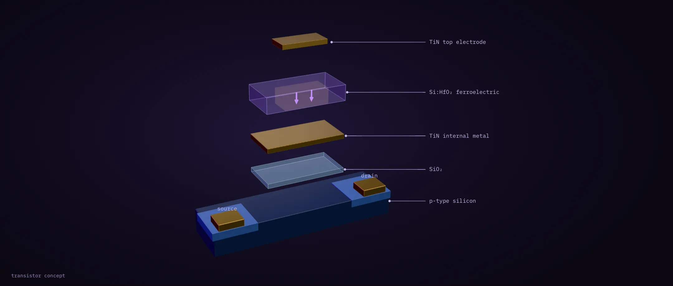
TiN / 13 nm Si:HfO₂ / TiN / 4 nm SiO₂ / p-Si
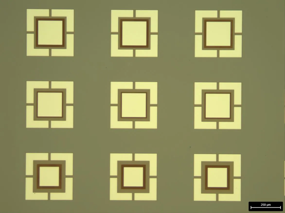
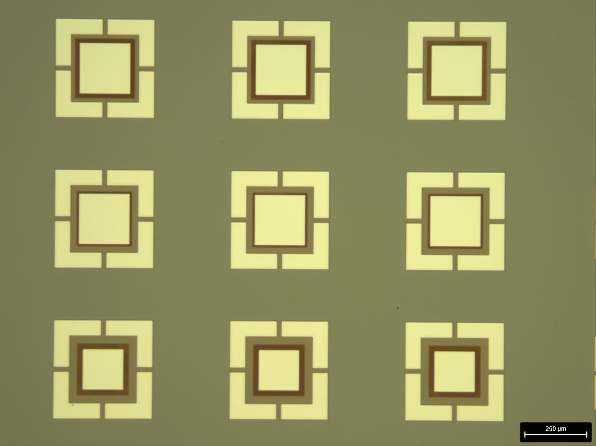
A metal layer between the ferroelectric and oxide separates the stack into two capacitors with an internal voltage node. Because capacitance scales with area, I varied the top-electrode area while keeping the other layers unchanged. The fabricated devices covered capacitance ratios from 1.0 to 2.6.
-
Fabrication and process development at CMi
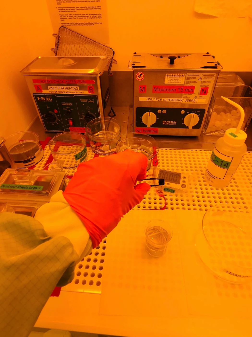
The process used sixteen wafer-level steps, followed by chip-level processing to limit the impact of a failed anneal. During TiN etching, I monitored reflectivity and stopped at about 13 s of a 30 s recipe. Resistance measurements helped identify electrode damage: 1.5 kΩ on a good chip and 5 kΩ on a damaged one.
-
Cryogenic characterisation below 77 K
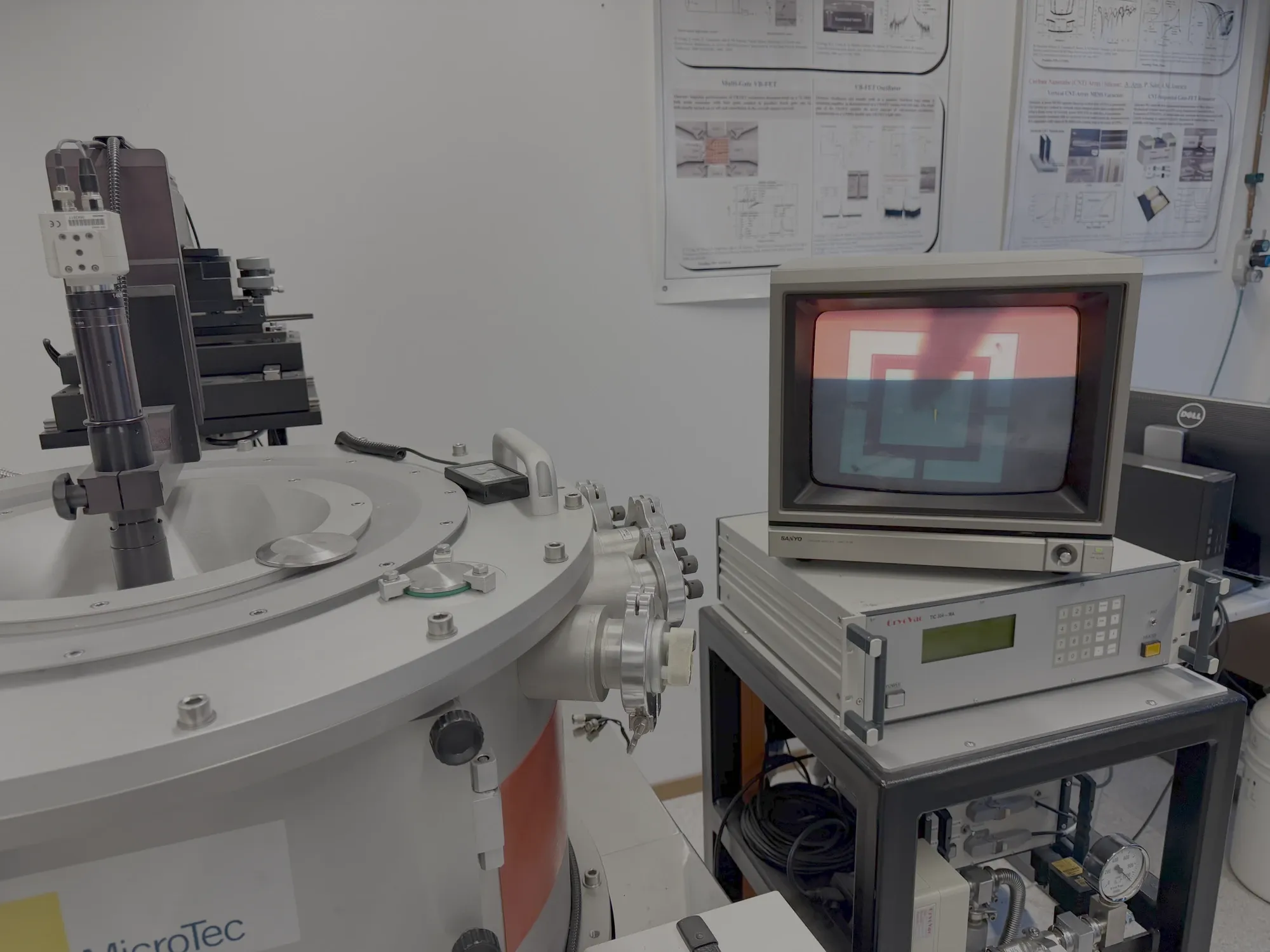
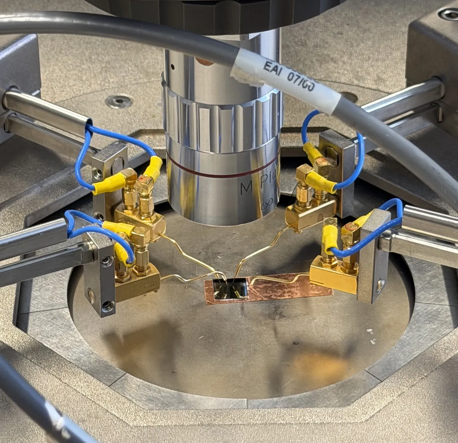
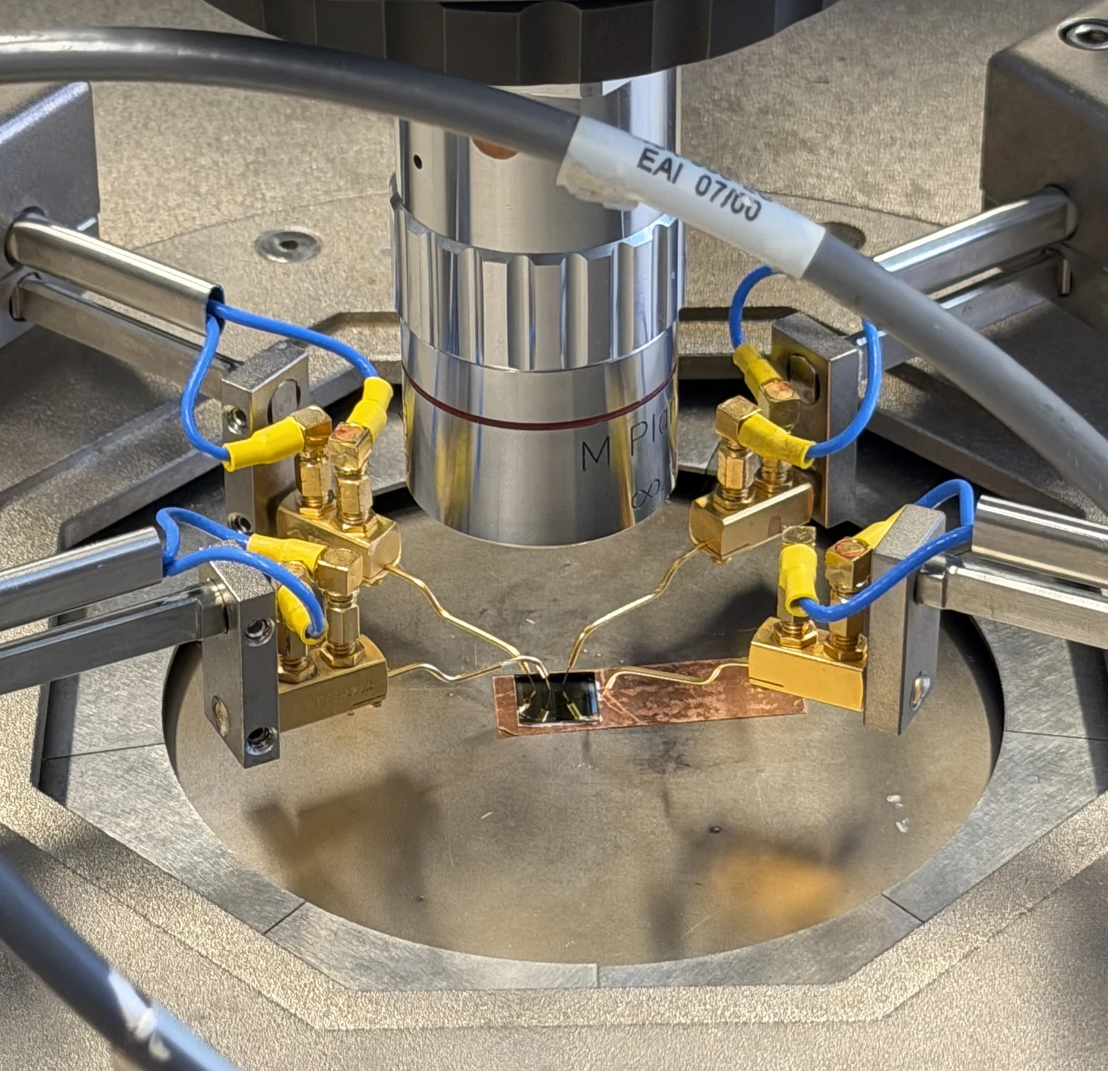
I measured individual devices on a cryogenic probe station below 77 K. The ferroelectric branch showed polarisation switching, with current peaks near the steep part of the reversal. These peaks increased with device area, consistent with a polarisation current rather than a response independent of electrode size.
-
Electrode area and internal electric field
1.3 → 2.0 MV/cm
As the capacitance ratio increased from 1.0 to 2.6, the inferred ferroelectric field rose from 1.3 to 2.0 MV/cm at 4 V. COMSOL predicted 1.8 to 2.5 MV/cm at 5 V. The measurements support using electrode area to tune the internal field, while the different applied voltages limit a direct numerical comparison.
-
Unresolved full-stack memory operation
The full stack showed a large hysteresis whose shape changed between 100 kHz and 1 Hz. Charge trapping can also cause hysteresis, so these measurements did not establish a common operating range for ferroelectric switching and channel control. My next test would hold the bias to examine relaxation and distinguish trapping from retained polarisation.
Ferroelectric field vs. capacitance ratio
The top electrode area changes the capacitance ratio and the division of gate voltage between the ferroelectric and oxide. Adjust the ratio and gate bias to compare the model with the two measurement-derived field values.
- Electrode area ratio AFE/ADE
- 0.30
- Voltage across ferroelectric
- 2.40 V
- Ferroelectric field
- 1.85 MV/cm
- Oxide field
- 4.00 MV/cm
- Depolarisation relative to ratio 1
- 0.80×
Full-switching threshold reached Within design window Oxide field below limit
Model equations
C = ε₀ε_r A / d: At fixed thickness and permittivity, capacitance depends on electrode area.V_FE = V_G · C_DE / (C_DE + C_FE): Voltage division between the two series capacitors.E_FE = V_FE / d_FE: Electric field across the ferroelectric layer.
Report values: εFE 28, εDE 3.9, dFE 13 nm, dDE 4 nm. Fabricated capacitance ratios: 1–2.6.
The model predicts higher fields than those inferred from the measurements. It treats the oxide branch as a constant capacitance, while the MOS capacitance changes with bias between accumulation and inversion. The reference points were obtained at 4 V gate bias.
My contribution
I modelled the stack, designed the electrode layouts, developed the cleanroom process and characterised the devices. Electrode area tuned the internal field.