
research · Sept 2026 – present
Time-resolved switching in two-dimensional ferroelectrics
My master’s thesis at MIT studies how polarisation switches in sliding ferroelectrics. Their fast, low-energy switching makes them candidates for the efficient memory that AI and neuromorphic computing need.
Project details
-
Sliding ferroelectricity
A parallel bilayer of boron nitride can be ferroelectric. Sliding one layer relative to the other by less than an ångström reverses its out-of-plane polarisation. Switching proceeds through the motion of a domain wall: as the wall moves across the device, the region behind it changes polarisation.
-
Domain-wall motion and measurement timescales
Published measurements apply a pulse and read the device afterwards, so they show where the wall stopped, not how it got there. The speed estimates also disagree: a few hundred micrometres per second from operando electron microscopy of a twisted bilayer, and about a thousand metres per second inferred from switching times in boron nitride.
-
Device dimensions for time-resolved measurements
I am exploring whether pinning helps explain the different reported speeds: a wall may move quickly between sites but spend longer waiting at them. With the oscilloscope’s 160 ps sampling, a wall moving one micrometre per nanosecond gives about six samples per micrometre. A twenty-micrometre bar would give over a hundred samples during one crossing.
-
Assembling the two-dimensional material stack
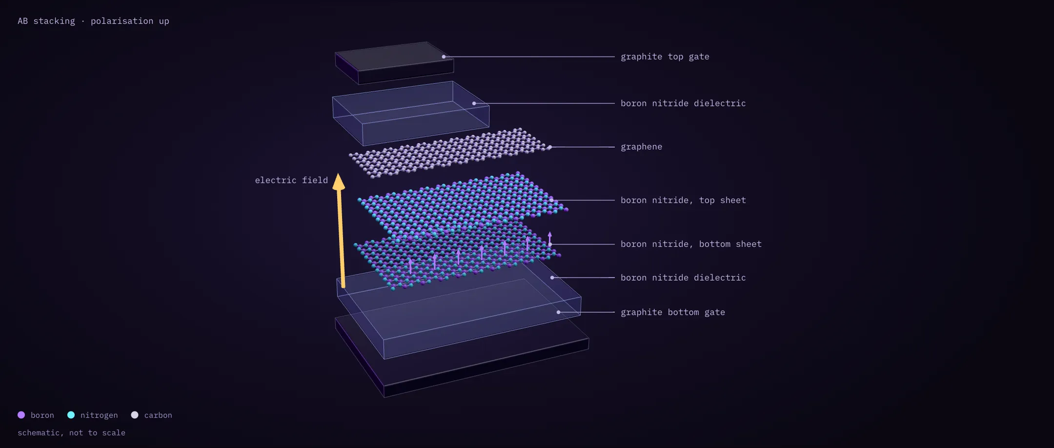
The device follows a published design: graphite gates, boron nitride dielectrics, a graphene sensor and the parallel bilayer. It is built by the published method: flakes are exfoliated with tape onto silicon chips and chosen under a microscope, then a polymer stamp picks up each layer in turn and lays the stack on the bottom gate.
-
Graphene edge contacts and device patterning
The published fabrication process defines the contacts by electron-beam lithography. A CHF₃/O₂ plasma exposes the graphene edge, followed immediately by chromium and gold deposition to form edge contacts. A second lithography and etching step patterns the long bar intended for the time-resolved measurement.
-
Reading the device during switching
The current readout measures the device seconds after a pulse, while the domain wall may cross it in nanoseconds. I am considering a fast buffer amplifier placed millimetres from the sample. It would allow measurement during the pulse and help preserve the signal on its way to the oscilloscope.
My contribution
I started this thesis in September 2026. I am developing the concept for a fast readout and the devices needed to resolve a single switching event. The work is at the concept stage; there are no results yet.